CONTENT
iCEDIP v0
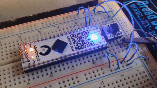
The iCEDIP puts a Lattice iCE5LP4K FPGA with its supporting circuitry on a semi-convenient, 40-pin DIP package!
Some batteries included. Metaphorically speaking.
This project was implemented in ~2019/09, with schematics originally redone for release in ~2021/02.
Features
- iCE5LP4K FPGA
- iCE40 Ultra Family
- ICE5LP4K-SG48ITR, (48pad QFN)
- Datasheet
- 3520 LUTs
- 80 kbits SRAM
- 1 PLL
- 2 I2C cores
- 2 SPI cores
- 10kHz and 48MHz oscillators built-in
- LED drivers
- Tested with iCE5LP1K and iCE5LP4K
- At the time of writing, this family seems to be unsupported by the open-source FPGA toolchains (icestorm).
- iCEcube2 is free, with yearly licenses.
- SPI Flash memory
- Various sizes can be installed
- Tested with:
- RGB LED
- Driven by FPGA-integrated drivers
- Integrated voltage regulators and rail switches
- Ensures somewhat less incorrect rail staging
- Single +3.3V supply operation possible
- Tie both VCIIOs to master +3.3V input
- Three IO banks
- One with fixed +3.3V VCCIO
- Two with separate VCIIOs
- 4-layer PCB
- 8-pin programming header
- Only supports programming of the external Flash(?)
- Probably not compatible with anything, mind the pinout.
Reference
IO Pinout
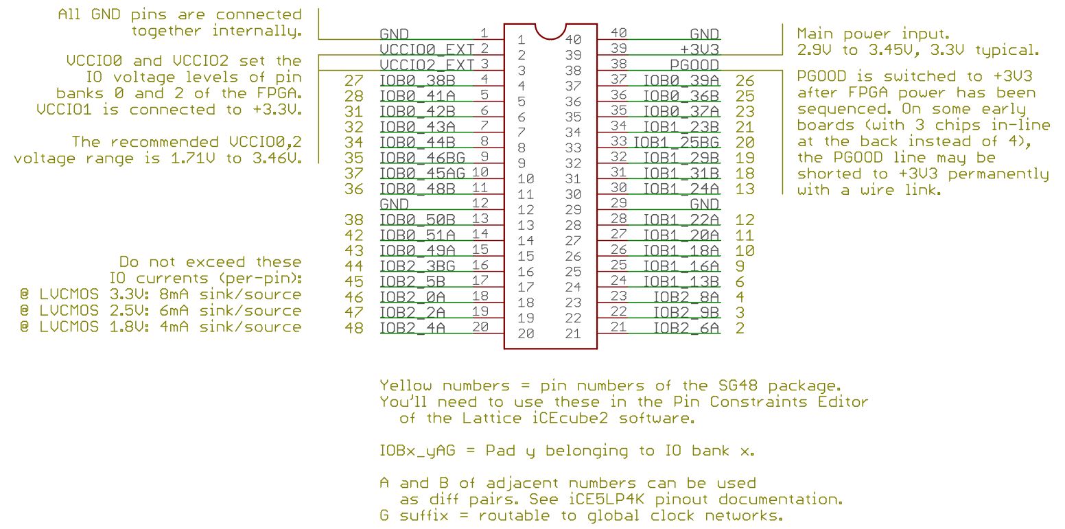
PGOODis shorted to+3V3on some (most) instances of iCEDIP, but is meant to be switched from +3V3 after successful power-up.VCCIO0andVCCIO2supply IO voltage toIOB0_*andIOB2_*pins respectively.IOB1_*pins are always use+3V3IO voltage.
Programming Header Pinout
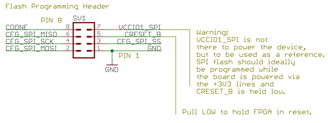
Pin 1 is shown by a <1 symbol on the PCB.
CFG_SPI_*signals connect to the SPI flash.CRESET_Bdriven low resets the FPGA.- DO NOT feed power to
VCIIO1_SPI. This line is only meant as a reference line for the programmer’s buffers. CDONEis pulled low by the FPGA during configuration load and in case of configuration failure. See the relevant datasheets.
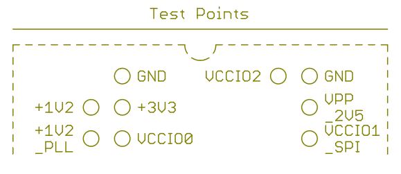
Test Points
There is a handful of test points for measuring rail voltages. This is useful especially during initial bring-up.
Schematic
A nice schematic with useful reference notes can be found below:
Funny tidbits & Lessons learned
- One can flash iCE5LP1K devices with iCE5LP4K firmware
- Yet, both devices seem to work the same? >:/
- There’s a ~3€ price difference!
- ICE5LP1K-SG48ITR : ~4.75€ (1 qty @ eu.mouser.com)
- ICE5LP4K-SG48ITR : ~7.55€ (1 qty @ eu.mouser.com)
- The CFG LED doesn’t quite work right
- Dimly lit after successful firmware load
- Not lit when firmware loading failed
- It was intended to serve as a user-programmable LED
- Sadly, it seems that the CDONE pin is unusable as a GPIO, even though the family datasheet (but not the pinout specs) seem to mention otherwise. Bummer.
- It was intended to add a NPN buffer for the CDONE pin, so the LED isn’t driven directly from the CDONE pin. This was forgotten about before the boards were produced. Surprisingly, this doesn’t seem to have any ill-effects so far.
- The RGB LED is too damn bright even at minimum current.
- The LED part used here is Lite-On LTST-C19HE1WT.
- “1616” footprint, common-anode.
- Power staging is important.
- Staging the power supply wrong will result in the FPGA “crowbarring” the rails.
- The staging on this board only counts with power-up staging.
- No special handling for power-down is handled. This isn’t exactly kosher.
- This may result in “crowbarring” after a deeper brownout.
- The “crowbarred” FPGA may still continue to operate “normally”, while heating itself up quite badly.
- MLCCs seem to like to appear shorted, sometimes.
- During the assembly of some prototype boards, it was found that many MLCCs would appear shorted.
- Not sure if this was caused by the MLCCs themselves, or solder wicking under the package.
- This was magically resolved by touching up the MLCCs with a soldering iron and reflowing them this way. The short was gone, and the MLCCs appeared normal again.
More shenanigans
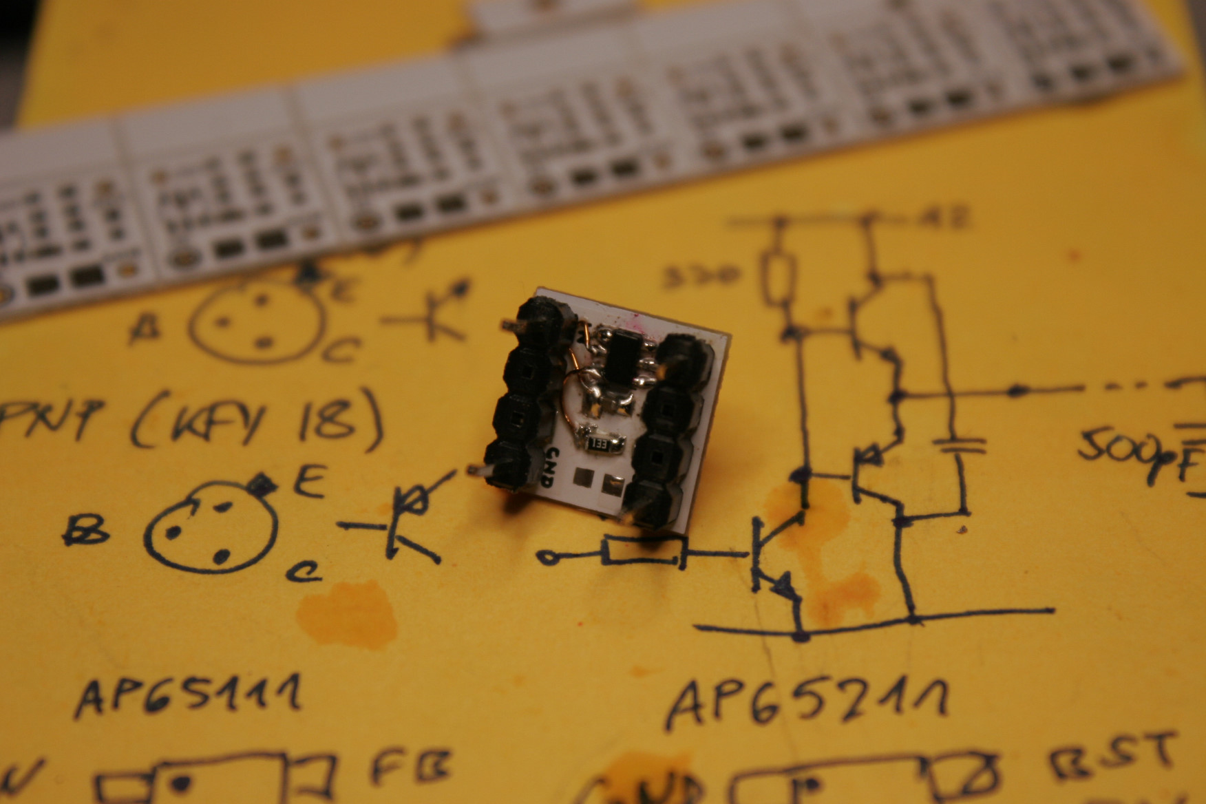
To power these FPGA boards, I have also designed some small DIP8-sized buck regulator modules.
These can be configured to output 3.3V, or about any other voltage from 0.8V to Vin.
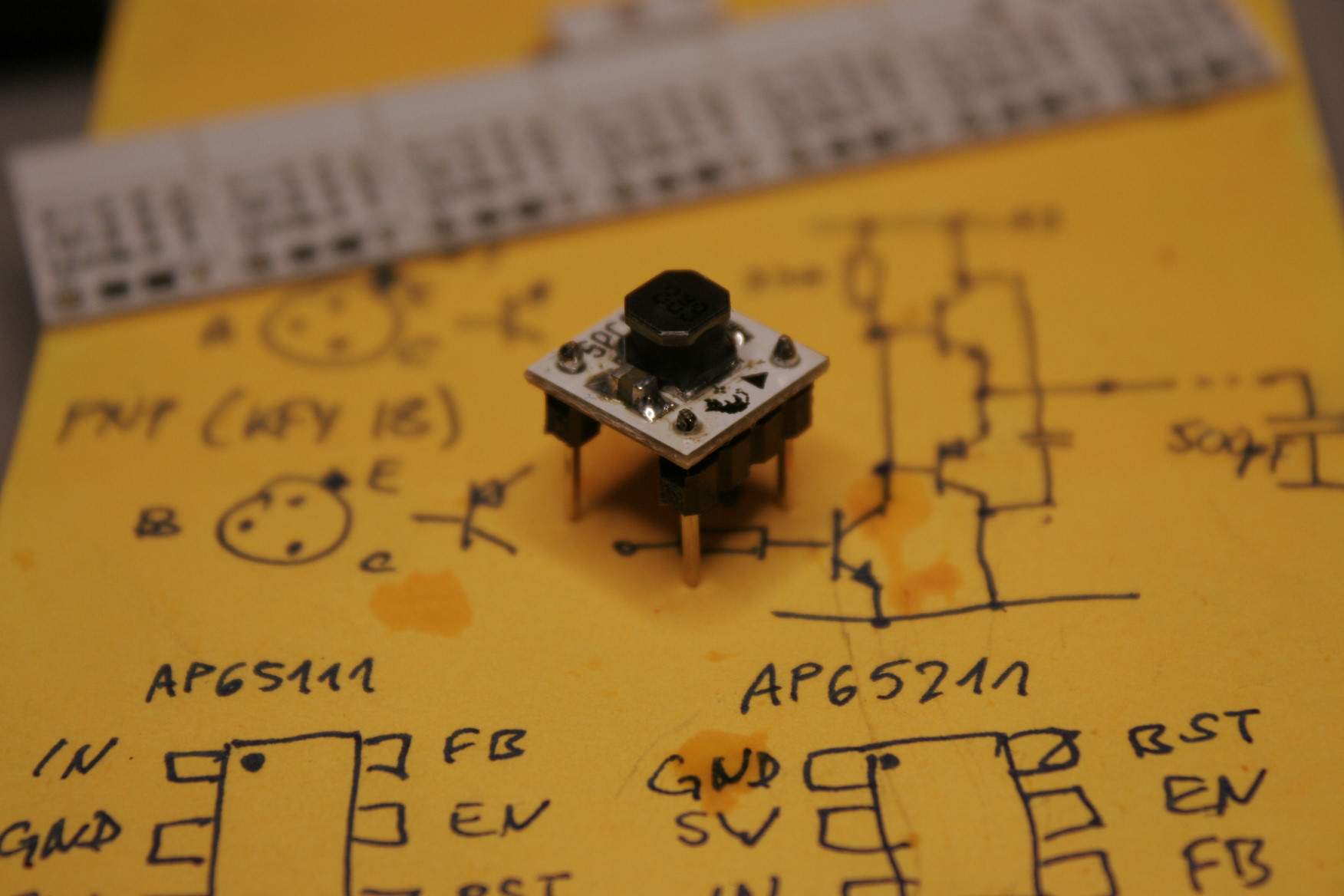
Sadly, I have designed these around the AP65111 chip, which has since somehow gone out of production and is now not recommended for new designs (NRND), sometime after I’ve designed the PCBs around it and got around to ordering them.
The AP65211 and AP65211A have since been introduced as replacements, however, both have incompatible pin-out to the AP65111, and both have since been marked as NRND, without direct replacement.
I have still managed to shoehorn the AP65211 onto the board designed for A65111, flipping it over and rewiring some pins… It doesn’t work quite as well as it should, but it works well enough.
Perhaps I’ll redesign this for some other switcher chips later…